InnoMemory, LLC has launched a sweeping litigation campaign, asserting Patent US7057960B1 against various companies across multiple industries. With 73 total cases – 44 inactive and 29 still active – this patent has been at the center of legal battles involving banks, technology firms, and major corporations such as American Airlines, National Instruments, and Alliance Bank. The scale of this enforcement effort raises an important question: How strong is this patent, and could related patents challenge its validity?
This patent, originally assigned to Cypress Semiconductor Corp., relates to power-efficient memory refresh operations, a critical function in modern electronic systems. However, in high-stakes litigation, related patents can play a decisive role, potentially limiting the patent’s claims or leading to invalidation.
That is where Global Patent Search (GPS) becomes an essential tool. By identifying related patents, GPS enables legal teams to evaluate whether the patented invention was truly novel at the time of filing. In the following analysis, we will examine the core features of Patent US7057960B1 and assess five related patent references that could impact its enforceability in court.
Understanding Patent US7057960B1
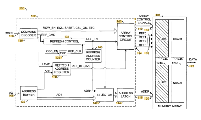
Patent US7057960B1, titled “Method and architecture for reducing the power consumption for memory devices in refresh operations,” presents a technique for optimizing power efficiency in memory devices during background operations, particularly refresh cycles. Originally assigned to Cypress Semiconductor Corp., this patent describes a method that allows selective activation of memory sections during refresh operations, thereby minimizing power usage, especially in standby mode.
Source: Google Patents
Its four key features are:
#1. Selective memory refresh – The patent introduces a mechanism to refresh only specific sections of a memory array instead of the entire memory, reducing unnecessary power consumption.
#2. Periphery circuit control – The system activates only the periphery circuits associated with the memory sections undergoing refresh, leaving inactive sections untouched to save power.
#3. Programmable refresh addressing – A programmable address signal determines which memory sections undergo a refresh, enabling adaptive power management based on device requirements.
#4. Standalone and background operations – The architecture supports additional memory-related background operations, such as parity checking, while still focusing on reducing power consumption.
Patent US7057960B1 is significant in multiple litigations involving InnoMemory, LLC, against various entities, particularly in industries where power efficiency in memory operations is crucial. The patent’s claim of a novel approach to reducing standby power consumption may be challenged if other patents already implemented similar methods. As part of the litigation process, identifying related patents that disclose comparable memory refresh power-saving techniques could be critical in evaluating the patent’s validity.
Related Patent References for US7057960B1
#1. US20020147885A1
This patent, filed on April 5, 2001, describes a method for managing refresh operations in a pseudo-static memory. The invention introduces DRAM sub-arrays (matrices) divided into sections, allowing background operations, such as refreshes, to be performed selectively. The method optimizes memory power consumption by controlling refresh timing and reducing unnecessary operations.
Key Features of this Related Patent:
This reference discloses a memory structure that divides DRAM sub-arrays into sections and uses control signals to manage refresh operations. It also describes the ability to perform background operations in multiple sections independently, which aligns with the key aspects of US7057960B1. Additionally, the reference discusses power optimization strategies to reduce unnecessary refreshes, making it relevant for evaluating the novelty of the subject patent.
Which features of US7057960B1 are disclosed by US20020147885A1?
| Key Feature of Claim 1 | Disclosure Status |
| The memory array is divided into a plurality of sections | Fully Disclosed |
| Background operations in each section are controlled by control signals | Partially Disclosed |
| Background operations can be enabled simultaneously in two or more sections independently | Fully Disclosed |
| The method reduces power consumption during background operations | Partially Disclosed |
Key Excerpt from US20020147885A1:
“In this first embodiment, the address of the row to be refreshed is supplied from a standard refresh counter, labeled RC(global) in FIG. 2, during every DRAM access cycle that causes a read (or write) miss. As shown, when DSA1 detects a miss, a refresh command is issued to the corresponding sub-array.”
#2. US20020048208A1
This patent, filed on October 9, 2001, describes a semiconductor device with a memory cell array divided into multiple sections, enabling controlled refresh operations to optimize power consumption. The invention introduces block controllers that manage refresh signals independently for different memory sections, allowing background operations to be performed selectively. The method also includes mechanisms to reduce refresh cycles when the device is in a power-saving state.
Source: GPS
Key Features of this Related Patent:
This reference discloses a memory array divided into multiple sections and describes control signals managing refresh operations for each section. It also discusses independent background operations in different memory blocks and details methods for reducing power consumption during refresh cycles. These aspects align with the key claims of US7057960B1, making this reference relevant for related patent analysis.
Which features of US7057960B1 are disclosed by US20020048208A1?
| Key Feature of Claim 1 | Disclosure Status |
| The memory array is divided into a plurality of sections | Fully Disclosed |
| Background operations in each section are controlled by control signals | Partially Disclosed |
| Background operations can be enabled simultaneously in two or more sections independently | Fully Disclosed |
| The method reduces power consumption during background operations | Fully Disclosed |
Key Excerpt from US20020048208A1:
“According to this embodiment of the present invention, since the number of refreshing operations when the semiconductor device is in an externally inaccessible state (power saving state, for example) can be reduced, the power consumption of the device can be effectively suppressed.”
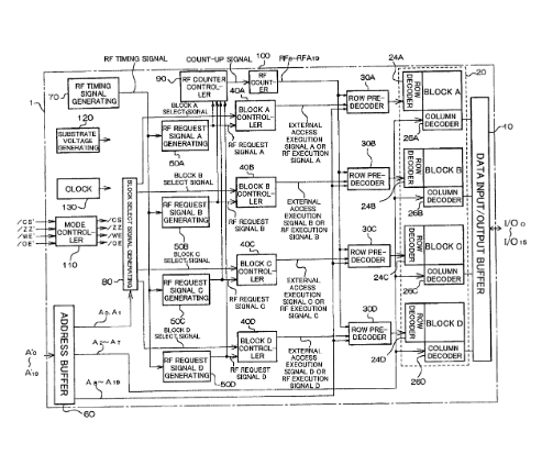
#3. US20020057607A1
This patent, filed on October 15, 2001, describes a semiconductor memory device with a memory array divided into multiple sections, each controlled by block controllers that manage refresh and background operations. The invention focuses on activating word lines efficiently, allowing for simultaneous operations in multiple sections while reducing power consumption during refresh cycles.
Key Features of this Related Patent:
This reference discloses a memory architecture divided into multiple sections and details control signals managing background operations in each section. It also describes the ability to enable background operations simultaneously in multiple sections and presents control signals and decoded address signals to periphery circuits. Additionally, the reference discusses techniques for reducing power consumption by optimizing refresh cycles, making it relevant for assessing the validity of US7057960B1.
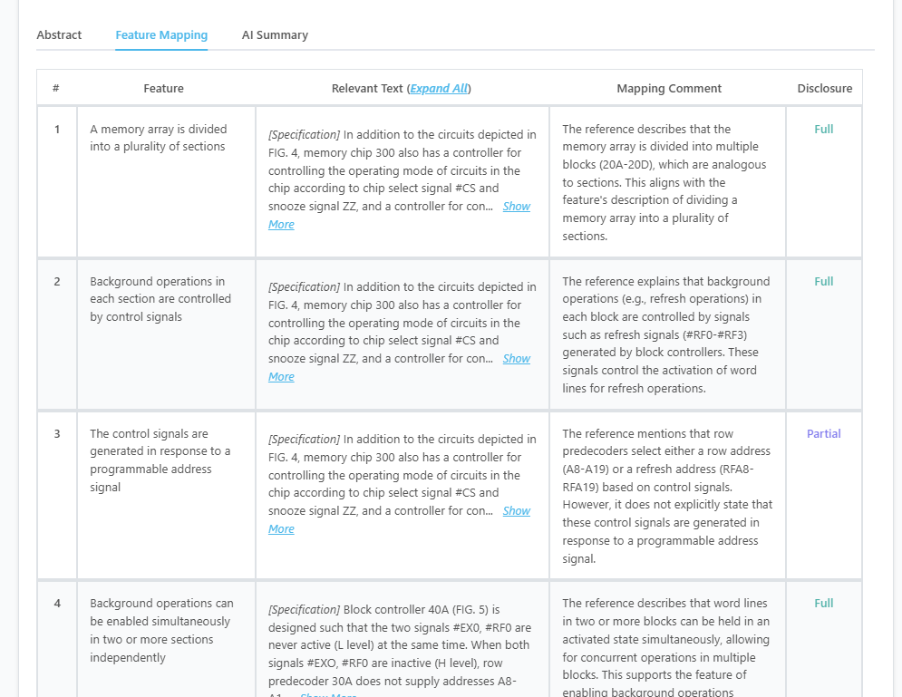
Here’s what the mapping from the tool for this particular patent looks like:
Source: GPS
Which features of US7057960B1 are disclosed by US20020057607A1?
| Key Feature of Claim 1 | Disclosure Status |
| The memory array is divided into a plurality of sections | Fully Disclosed |
| Background operations in each section are controlled by control signals | Fully Disclosed |
| The control signals are generated in response to a programmable address signal | Partially Disclosed |
| Background operations can be enabled simultaneously in two or more sections independently | Fully Disclosed |
| Control signals and decoded address signals are presented to periphery array circuits of the sections | Fully Disclosed |
| The method reduces power consumption during background operations | Fully Disclosed |
Key Excerpt from US20020057607A1:
“The word line activation controller herein can perform refresh operations in the semiconductor memory device, and also obviates the need to repeatedly activate and deactivate word lines in each cycle during periods in which no memory access occurs, thereby reducing power consumption.”
#4. US6415353B1
This patent, filed on September 24, 1999, describes a semiconductor memory system where memory cells are arranged in independently controlled memory banks. The invention allows simultaneous read, write, and refresh operations within separate banks, optimizing performance and reducing power consumption. The system also includes a refresh address generator and a central refresh timer to coordinate memory operations efficiently.
Key Features of this Related Patent:
This reference discloses a memory array divided into independently controlled sections (memory banks) and describes control signals managing background operations in each section. It also supports simultaneous background operations in multiple sections and details techniques to reduce power consumption during refresh cycles. These features align with the key claims of US7057960B1, making this reference relevant.
Which features of US7057960B1 are disclosed by US6415353B1?
| Key Feature of Claim 1 | Disclosure Status |
| The memory array is divided into a plurality of sections | Fully Disclosed |
| Background operations in each section are controlled by control signals | Fully Disclosed |
| The control signals are generated in response to a programmable address signal | Partially Disclosed |
| Background operations can be enabled simultaneously in two or more sections independently | Fully Disclosed |
| Control signals and decoded address signals are presented to periphery array circuits of the sections | Partially Disclosed |
| The method reduces power consumption during background operations | Fully Disclosed |
Key Excerpt from US6415353B1:
“Accordingly, the present invention provides a memory device that includes a plurality of memory cells that must be periodically refreshed in order to retain data values, and a control circuit for accessing and refreshing the memory cells, while reducing power consumption during these background operations.”
#5. US6385113B1
This patent, filed on April 30, 1999, describes a method for operating an integrated circuit with a sleep mode to reduce power consumption. The invention introduces a memory architecture divided into multiple sections (banks), where a refresh controller controls selective refresh operations. The method optimizes memory power usage by enabling sleep modes and selective refreshing of active memory sections while minimizing refresh cycles in inactive sections.
Key Features of this Related Patent:
This reference discloses a memory array divided into multiple sections and describes control signals managing refresh operations. It also discusses power reduction techniques by enabling low-power sleep modes and selectively refreshing memory sections. However, it does not explicitly state that background operations can be enabled simultaneously in multiple sections or that control signals are generated in response to a programmable address signal, making its relevance to US7057960B1 partial in certain aspects.
Which features of US7057960B1 are disclosed by US6385113B1?
| Key Feature of Claim 1 | Disclosure Status |
| The memory array is divided into a plurality of sections | Fully Disclosed |
| Background operations in each section are controlled by control signals | Partially Disclosed |
| The control signals are generated in response to a programmable address signal | Partially Disclosed |
| Background operations can be enabled simultaneously in two or more sections independently | Partially Disclosed |
| Control signals and decoded address signals are presented to periphery array circuits of the sections | Partially Disclosed |
| The method reduces power consumption during background operations | Fully Disclosed |
Key Excerpt from US6385113B1:
“In many applications, such as hand-held, battery-powered devices, a low power mode is used to reduce the power consumption of the memory device. Sleep modes are desirable in such applications as they increase the battery life of the device while maintaining stored data integrity.”
Feature Comparison Table
| Key Feature of Claim 1 | US20020147885A1 | US20020048208A1 | US20020057607A1 | US6415353B1 | US6385113B1 |
| The memory array is divided into a plurality of sections | Fully Disclosed | Fully Disclosed | Fully Disclosed | Fully Disclosed | Fully Disclosed |
| Background operations in each section are controlled by control signals | Partially Disclosed | Partially Disclosed | Fully Disclosed | Fully Disclosed | Partially Disclosed |
| The control signals are generated in response to a programmable address signal | Not Disclosed | Not Disclosed | Partially Disclosed | Partially Disclosed | Partially Disclosed |
| Background operations can be enabled simultaneously in two or more sections independently | Fully Disclosed | Fully Disclosed | Fully Disclosed | Fully Disclosed | Partially Disclosed |
| Control signals and decoded address signals are presented to periphery array circuits of the sections | Not Disclosed | Not Disclosed | Fully Disclosed | Partially Disclosed | Partially Disclosed |
| The method reduces power consumption during background operations | Partially Disclosed | Fully Disclosed | Fully Disclosed | Fully Disclosed | Fully Disclosed |
How to Find Related Patents Using Global Patent Search?
Finding related patent is essential when evaluating a patent’s validity, particularly in litigation. The Global Patent Search (GPS) tool simplifies this process by providing comprehensive access to patent databases and advanced feature-matching capabilities.
Search by patent number or description – Enter a specific patent number or relevant technical keywords to retrieve related patents and publications.
Source: GPS
Leverage feature mapping – Compare the key features of the subject patent against existing references to identify overlaps.
Review matching results – Access a curated list of potential related patent references ranked by relevance.
Analyze detailed reports – Examine how each reference discloses specific elements of the patent claims.
Make confident decisions – Use data-driven insights to refine legal strategies and assess the strength of a patent’s claims.
By utilizing Global Patent Search, legal professionals and researchers can efficiently identify relevant related patents, improving the accuracy and effectiveness of patent validity assessments.
Take the Uncertainty Out of Related Patent Research

Navigating patent disputes requires thorough and precise related patent analysis. The Global Patent Search (GPS) tool simplifies this process by providing:
- Fast and efficient searches – Locate relevant patents quickly without the need for time-consuming manual research.
- Comprehensive feature mapping – Compare key elements of a patent with existing references to identify similarities.
- Reliable data insights – Strengthen your legal position with well-documented related patents that can impact patent validity.
Ensure you have the most relevant related patent references at your fingertips. Begin your search with GPS today.
Disclaimer: The information provided in this article is for informational purposes only and should not be considered legal advice. The related patent references mentioned are preliminary results from the Global Patent Search (GPS) tool and do not guarantee legal significance. For a comprehensive related patent analysis, we recommend conducting a detailed search using GPS or consulting a patent attorney.